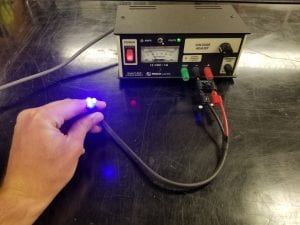
This demo illustrates one of the many uses of diodes through the light emission of various LEDs. It demonstrates the quantum mechanics behind diodes because the transition of electrons within can be seen in the form of photons in the visible light spectrum.
Materials:
- DC power supply – used to supply a fixed voltage to the provided LEDs.
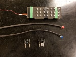
- LEDs – convert the supplied electrical energy into visible light of various frequencies.
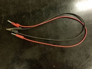
- Banana cables – connect the DC power to the given diodes.
Setup:
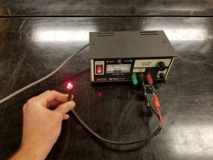
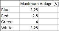
This diode demo requires the diodes to be plugged in directly to the 12V DC source one at a time to show their light emission properties. When applying the voltage, make sure that the voltage source knob is turned all the way down before turning on the source. Then slowly turn up the voltage until they turn on. One important note is that these diodes are fairly easy to burn out by applying too high a voltage. Below, in figures 5 through 7, is an example of the setup for each doide and its maximum voltage before burnout. To sumarrize these values, Figure 8 contains a chart of the maximum voltages to be applied to each diode. In addition, each diode must be hooked up in parallel with the provided resistor to prevent burnout.
The red diode shown above in Figure 5 is the most delicate. It produces a lower intensity of light so it can be tempting to turn up the voltage to produce a brighter beam. However, the maximum voltage for this assembly is 2.5 Volts.
The blue diodes shown in Figure 6 require a larger voltage, but produce a visibly increased intensity of the light emitted. The maximum voltage that should be applied to this setup is 3.25 Volts.
These white diodes in Figure 7 are very similar to the blue ones shown previously. As a result, they also have a maximum voltage of 3.25 Volts.
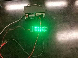
Figure 1 in the introduction shows the setup for the green diodes. This array has a maximum voltage of 4 Volts. The setup for this array slightly more complicated as it requires the use of the banana cables to attach the diodes to the DC source. For convenience, a table of maximum diode voltages is shown below in Figure 8.
Explanation:
To explain the quantum mechanics of the LED we must first understand the construction of a diode. To do this we need a quick review of the quantum mechanics behind insulators, conductors, and semiconductors. Below is a diagram showing the energy levels in each of these various materials towards the outer layer of their electron shells.
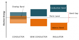
Figure 9: Electron energy levels for conductors, semiconductors, and insulators from ReasearchGate
The electron energy band gap in these materials helps us understand why they have their various properties. Conductors allow for a flow of electricity because their valence band electrons have an overlap with the band in which they can conduct. Insulators don’t allow for the flow of charge because the band gap between valence and conduction band is too large for electrons to jump. Semiconductors on the other hand offer a balance between these two extremes. With no external excitation, semiconductors act like insulators by allowing no charge flow. However, these electrons are easily excited into the conduction band by either thermal excitation or externally applied voltages. This versatility of semiconductors is why they are used so widely in electrical components, including the diode.
The base material for diode construction consists of some type of semiconductor, generally silicon. These pure silicon bases are then doped with a secondary material. This process involves adding impurities into the pure silicon lattice in the form of atoms with different chemical properties. The two most common doping types are P-type and N-type.
In N-type doping, atoms are injected into the silicon lattice which have five valence electrons, as opposed to silicon’s four. This has the effect of adding an additional electron which can flow in the conduction band. One common example of this is N-type doping with Phosphorus with its five valence electrons. This type of doping gets its name because the charge carrier of this material, the electron, is negative.
P-type doping is similar to N-type, except that in this case the injected atoms have three valence electrons. This creates the absence of an electron in silicon’s otherwise uniform lattice of four valence electrons. To visualize this, the absence of electron is called a hole, and referred to as a positively charged object which can travel through the lattice. The charge carrier of this material is the positively charged hole, hence the name P-type doping.
We then stick these two materials together to make a diode or a PN junction as shown below in Figure 10.

Figure 10: Diode Diagram from Wikipedia
When first connected, the excess electrons and holes are at very high concentrations on either side. These charges will diffuse to create an electric field at the central junction of the device as shown below.
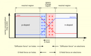
Figure 11: Diode equilibrium from Wikipedia
This device is then typically connected to an electrical circuit as shown in Figure 9 above. To allow current flow through this device, an external voltage must be applied to overcome the internal electric field created by the charge carriers at the center of the device. Another way to visualize this flowing current is as the injection of electrons into the device.
Electrons are injected into the N-type side where they continue to flow into the central region, then recombine with the abundant holes in this area. This particular part of the process is what we’re interested in when describing the function of light emitting diodes, or LEDs. When the electrons are injected into the N-type material they are in the conduction band energy level. Meaning that the valence band is full as shown in Figure 9.
These electrons flow through the conduction band as they cross through the N-type region. Then they approach the large concentration of holes at the central depletion region. These positively charged holes will reside in the valence band because they represent the lack of an electron in the lattice. Once a free electron in the conduction band approaches a hole in the valence band they will attract due to the opposing charge. They then go through electron-hole recombination,in which a free electron steps down in energy to fill the empty spot in the valence band lattice. This electron transitioned from a higher energy state down to a ground state.
By conservation of energy, we expect that this energy must be converted into some other form. In fact, this energy is emitted as a photon having a wavelength corresponding to its energy level from,
It is this phenomenon that is used in the creation of LEDs. One important note is that the emitted photons won’t always be in the visible light spectrum. Due to this, it is important to keep the energy band gap between conduction and valence bands in mind when making an LED. The device will only emit visible light if a change in energy between the two bands corresponds to a photon with a wavelength in the visible light spectrum. So now we can see that LEDs are simple diodes whose energy band gap has been adjusted so that electrons transitioning across it will produce a photon visible to our eyes.
Written by Noah Peake
