Figure 1: Photovoltaic cell demo version 2
Equipment:
Version 1:
- Photovoltaic cell connected to LED lights [Cabinet F2]
- One strong light source
- Projector [Below cabinet H]
- Carbon arc lamp [Lower cabinet below central tables]
- Lamp powered by variac [Cabinet E3 and cabinet K4 respectively]
Version 2:
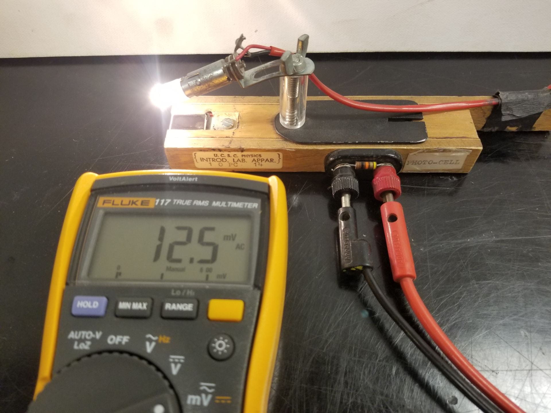
- Digital volt meter [Counter below cabinet J, or in cabinet F2]
- Photo cell apparatus [Cabinet F2]
- Pasco DC power supply (model Pl-9596) [Cabinet K2]
- Video camera (for larger classes)
Demo:
Version 1:
Plug in and turn on the projector or other powerfull light source. Then, pass the photovoltaic (PV) cell over the strong light source to collect some of its energy. This collected energy is then used to light up the LED panel, which can be shown to students even in large classrooms.
Version 2:
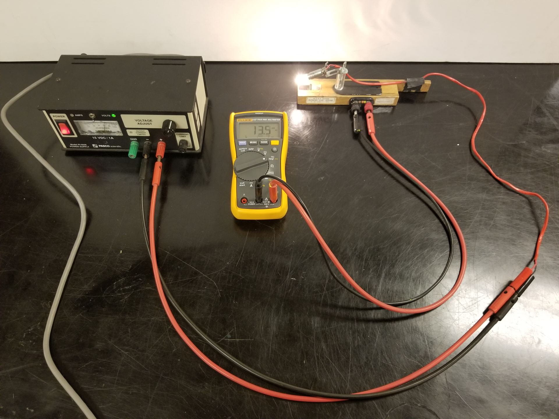
Figure 2: Photovoltaic cell demo setup, version 2
Begin setup by making the banana jack connections shown in Figure 2 above. Next, set the digital volt meter (DVM) to the voltage reader setting on the milivolt scale. Finally, turn on the Pasco supply and apply a voltage to the light bulb. Varying the voltage applied to the light bulb will change the energy collected by the PV cell, which is shown by the voltage on the DVM. Don’t exceed 12 volts with the Pasco supply or else the light bulb will burn out.
Explanation:
Photovoltaic (PV) cells are electronic devices that generate electricity when light falls on them. This is achieved through several layers of semiconductors designed to capture this light. Both layers begin as a pure semiconductor crystal such as silicon or germanium. Then, these layers are doped to add impurities into the crystalline structure. This serves to provide either free electrons within the lattice unbound to atoms, or holes which are an absence of an electron in the lattice. Materials with excess electrons are referred to as n type material, while those with excess holes are called p type. When these two materials are combined in a PN junction, they form the basic makings of a PV cell. An example of this can be seen below in Figure 3.
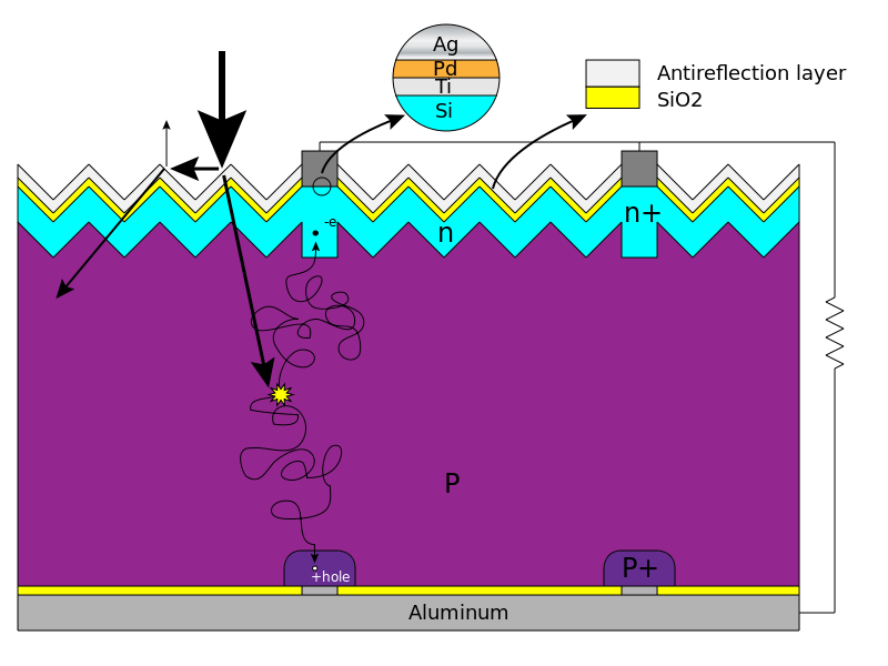
Figure 3: Cross-section of PV cell, from Wikipedia
The basic PN junction configuration can be seen above. In addition to the PN junction, the diagram shows an antireflective coating to increase the number of photons entering the cell, and electrodes to extract any energy produced.
With both p type and n type material joined, it becomes possible to collect the energy from incoming photons. The photons pass through the n type material from above and travel into the p type. Here the photon exchanges its energy with an electron. This electron becomes excited, dislodges from it’s parent atom, and is able to freely conduct. In other words, an electron hole pair has been created using the photon’s energy. Then the electron drifts upward toward the n electrode, and the hole drifts down towards the p electrode. Once they reach the electrodes, they create a usable current. This current can be used to power electronics such as the LEDs provided with this demo.
This is a property of the photoelectric effect. When light shines on a metal surface, electrons are emitted from the surface. A photo cell is an evacuated glass tube that has a piece or many pieces of metal and electrodes. When light shines on the metal it emits electrons and an induced currant flows through the circuit. In this case, it produces enough energy to power the LEDs.
Notes:
- An oscilloscope can be used in place of the DVM to show the voltage change over a long timescale
- In this setup, both input voltage from the Pasco supply and output voltage from the PV cell could be plotted side by side over time
- Voltage to the light bulb shouldn’t exceed 12 V
Written by Noah Peake